Here, we are going to learn about how TPUs work, how they are networked together to enable multi-chip training and inference and how this affects the performance of our algorithms
What is a TPU?
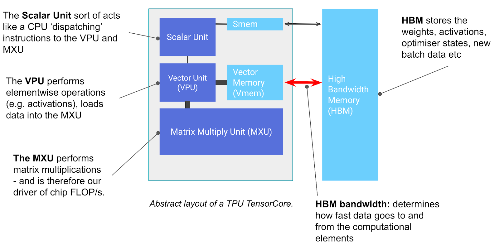
We can think of this TensorCore as a essentially just a really good matrix multiplication machine but it has some other functions too. The TensorCore has three key units:
-
The MXU(Matrix Multiply Unit) is the core of the TensorCore. On TPU7x, it performs one
bf16[8,256] @ bf16[256,256] -> f32[8,256]matrix multiply every4cycles using a systolic array (see Appendix B for details)- This is about
5.8e14bf16 FLOPs/s per MXU at 2.2GHz on TPU7x. Each TPU7x chip has 2 TensorCores, and each TensorCore has 2 MXUs, so the total bf16 FLOPs/s for TPU7x is around2.3e15. - TPUs also support lower precision matmuls with higher throughput (e.g. each TPU7x chip can do
4.6e15fp8 OPs/s).
- This is about
-
The VPU(Vector Processing Unit) performs general mathematical operations like ReLU activations or pointwise addition or multiplication between vectors. Reductions (sums) are also performed here. Appendix A provides more details.
-
VMEM (Vector Memory) is an on-chip scratchpad located in the TensorCore, close to the compute units. It is much smaller than HBM (for example, 128 MiB per chip on TPU7x vs 192 GiB of HBM) but has a much higher bandwidth to the MXU. VMEM operates somewhat like an L1/L2 cache on CPUs but is much larger and programmer-controlled. Data in HBM needs to be copied into VMEM before the TensorCore can do any computation with it.
-
HBM (High Bandwidth Memory) is a big chunk of fast memory that stores tensors for use by the TensorCore. HBM usually has capacity on the order of tens to hundreds of gigabytes (for example, the HBM capacity of TPU7x is 192GiB).
- When needed for a computation, tensors are streamed out of HBM through VMEM (see below) into the MXU and the result is written from VMEM back to HBM.
- The bandwidth between HBM and the TensorCore (through VMEM) is known as “HBM bandwidth” (around 7TB/sec for TPU7x) and limits how fast computation can be done in memory-bound workloads.
Here’s an example of how you might perform an elementwise product from HBM:
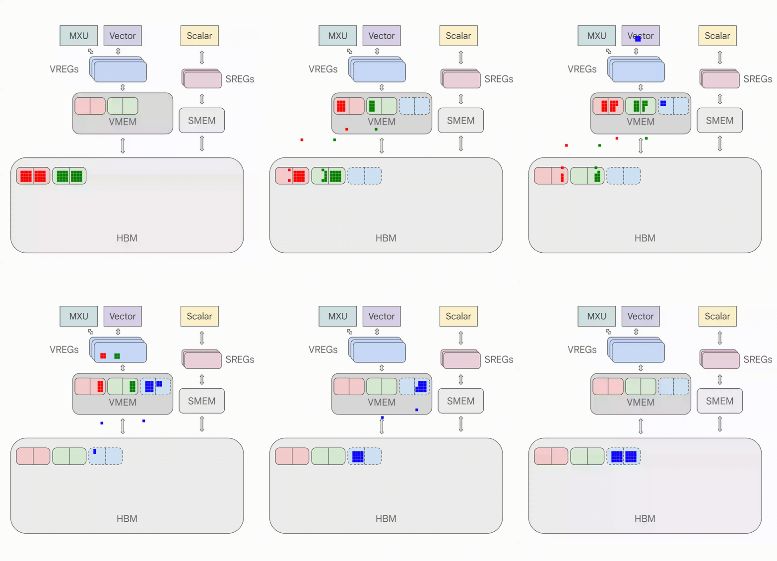
A matmul would look almost the same except it would load into MXU instead of VPU or Vector unit.
You can see chunks of data streaming into VMEM, then into the VREGs (vector registers), then into the Vector Unit, then back into VMEM and HBM. As we’re about to see, if the load from HBM to VMEM is slower than the FLOPs in the Vector Unit (or MXU), we become “bandwidth bound” since we’re starving the VPU or MXU of work in source
VMEM and Arithmetic Intensity
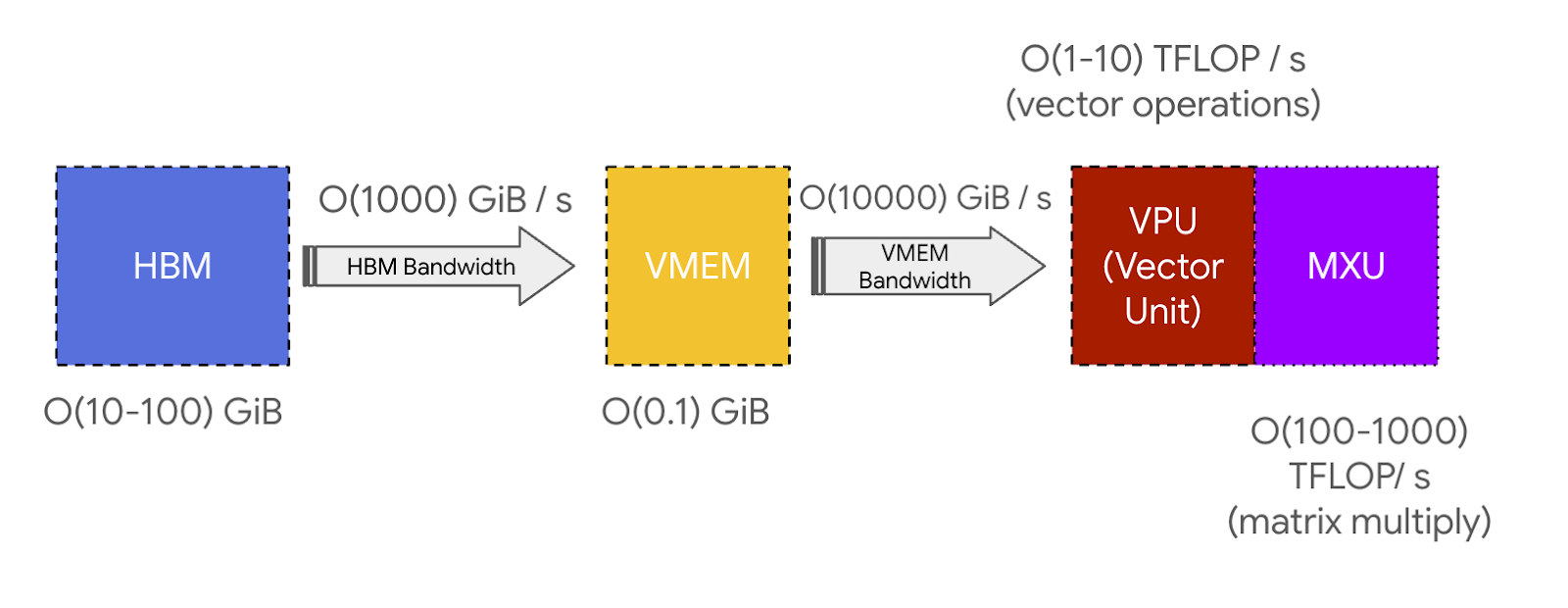
VMEM is much smaller than HBM but it has a much higher bandwidth to the MXU in source
As we know VMEM is much faster as compared to HBM, that means if we can fit our weights into VMEM instead of HBM, we can get the highest FLOPs possible. This means we can get this FLOPs at a much smaller batch sizes. This means we can make lower arithmetic intensity algorithms to perform efficiently but the challenge is that VMEM memory is so small
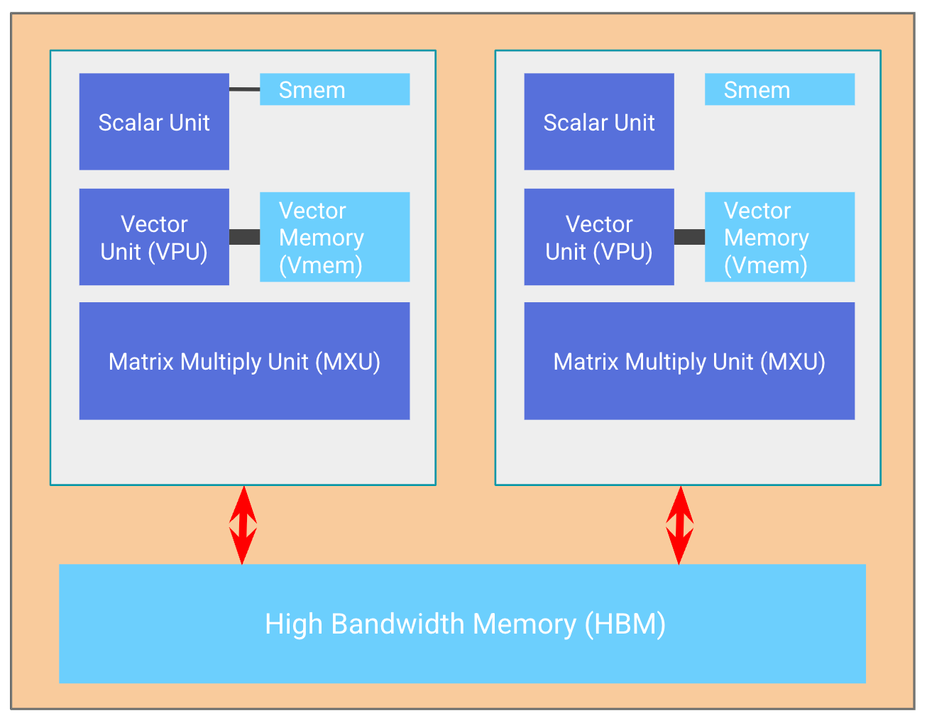
A TPU chip typically (but not always) consists of two TPU cores which share memory and can be thought of as one large accelerator with twice the FLOPs (known as a “megacore” configuration) in source
Chips are arranged in sets of 4 on a ‘tray’ connected to a CPU host via PCIe network. in source
For inference chips like the TPU v6e, we have 2 trays per host, instead of 1, but also only 1 core per chip, giving us 8 chips = 8 cores in source
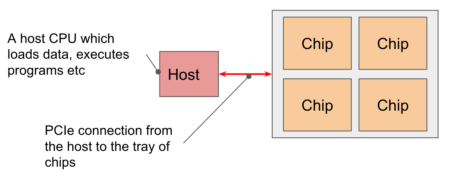
PCIe bandwidth is limited: Like the HBM ↔↔ VMEM link, the CPU ↔↔ HBM PCIe connection has a specific bandwidth that limits how quickly you can load from host memory to HBM or vice-versa. PCIe bandwidth for TPU v4 is 16GB / second each way, for example, so close to 100x slower than HBM. We can load/offload data into the host (CPU) RAM, but not very quickly. in source
TPU Networking
Chips are connected to each other through the ICI(Inter-Chip Interconnects) network in a Pod in source